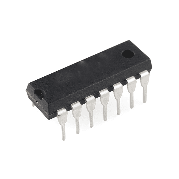
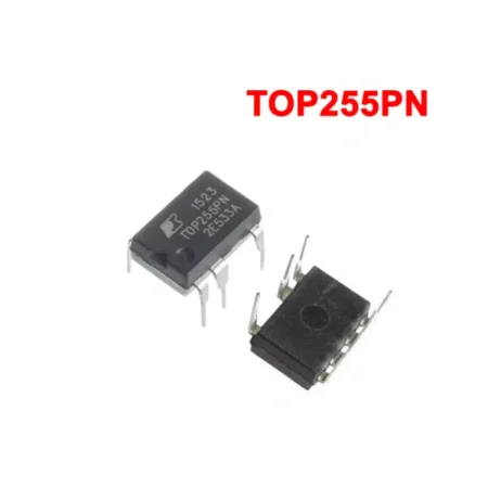
| Description: The 7491 packages an 8-bit shift register. Data present on the input pins will be clocked in to the first register once the circuit receives a clock pulse. All other data, already registered, will be shifted over to make room for the new input. Data at the far end of the chain will be clocked out every cycle. In this regard, this circuit acts as an 8 bit First-In-First-Out buffer queue.Multiple packages can be cascaded to form registers of varying lengths. To avoid propagation delays, multiple packages should be synchronously combined with proper extern control circuitry to minimize glitchy delays which will accumulate at each stage.  |
|
| View Datasheet Immediately – CLICK HERE |
7491 (8-Bit Shift Register (Serial Input / Serial Output))
36.00 EGP
Buy Now

