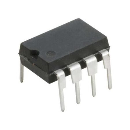

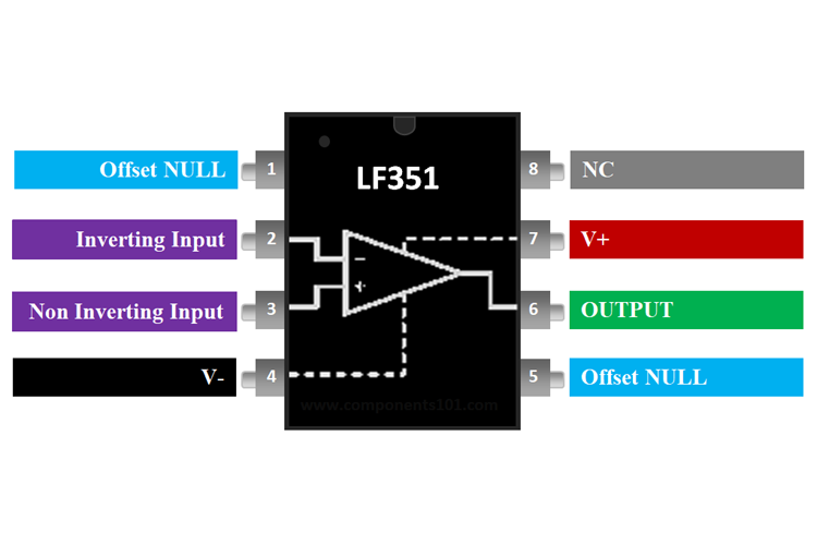
LF351 Pin Configuration
| Pin No. | Pin Name | Description |
| 1. | Offset Null 1 | The pin is used to remove the offset voltage and balance input voltage. |
| 2. | Inverting Input | Inverting signal Input |
| 3. | Non-inverting Input | Non-inverting signal Input |
| 4. | VEE | Negative Supply Input (Ground) |
| 5. | Offset Null 2 | The pin is used to remove the offset voltage and balance input voltage. |
| 6. | Output | Output of op-amp |
| 7. | VCC | Positive Supply Input |
| 8. | N.C. | Not Connected |
Features
- Low power consumption
- Output short-circuit protection
- High slew rate 13 V/us
- Low input-bias and offset current
- Latch-up free operation
- Internal Frequency Compensation
Technical Specifications
- Voltage Supply: ±18V
- Input Supply range: ±15V
- Differential Input Voltage: ±30V
- Input Offset Voltage: 3mV
Note: Complete technical information can be found in the LF351 Datasheet linked at the bottom of this page.
Where to Use LF351 IC?
LF351 is a single operational amplifier with an internally compensated input offset voltage. It also provides wide bandwidth, low input bias current, and offset current. Basically, LF351 is used in circuits that need high input impedance, high-speed integrators, Quick digital to analog converters, sample and hold circuits, etc.
How to Use the IC?
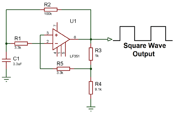
The below circuit diagram is used to generate the square wave, by adding a few resistors and capacitors externally. It is like a Schmitt trigger circuit in that the reference voltage for the comparator action depends on the output voltage. To find the value of the output frequency use the formula mentioned below:
FOSC = 1 / 2RFCF
Applications
- Square Wave oscillator
- High Q Notch Filter
- Sample and Hold Circuit
- Fast Digital to Analog Converters
- High Seed Integrators