
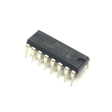

CD4015 – Two 4-bit Shift Registers
The CD4015 is a CMOS IC with two 4-bit shift registers. Each shift-register has serial input and parallel output pins. It’s commonly used to give you more output pins from a microcontroller, such as Arduino.
You’ll see an example of this further down.
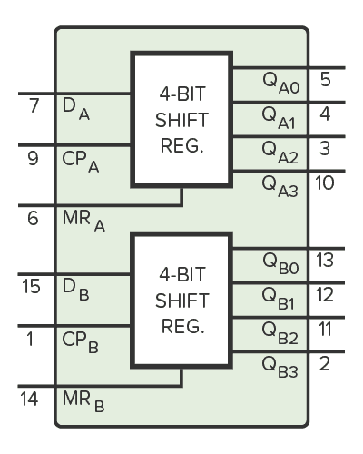
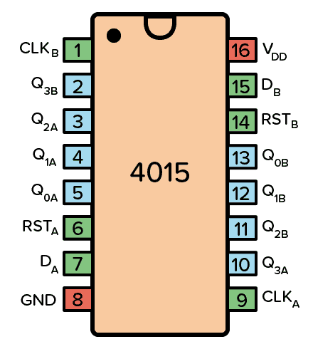
Pin Overview
| PIN NAME | PIN # | TYPE | DESCRIPTION |
|---|---|---|---|
| VDD | 16 | Power | Supply Voltage (+3 to +15V) |
| GND | 8 | Power | Ground (0V) |
| DA | 7 | Input | Data pin for register A |
| CLKA | 9 | Input | Clock pulse for register A |
| RSTA | 6 | Input | Reset pin for register A |
| QA0,QA1,QA2,QA3 | 5,4,3,10 | Output | 4-bit output for register A |
| DB | 15 | Input | Data pin for register B |
| CLKB | 1 | Input | Clock pulse for register B |
| RSTB | 14 | Input | Reset pin for register B |
| QB0,QB1,QB2,QB3 | 11,12,13, 2 | Output | 4-bit output for register B |
What is a 4-Stage Shift Register?
A shift-register is a simple memory circuit that can store a number of bits. You can build one using a series of flip-flops. Each flip-flop can store one bit. A 4-bit shift register like the ones in the CD4015 chip has 4 flip-flops and is often called a 4-stage shift register:
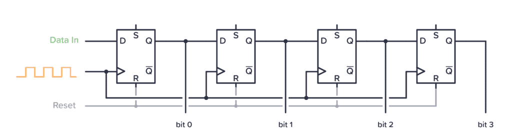
After the first clock pulse, whatever is on the Data In pin will be stored in the first flip-flop. What was on the first flip-flop from before is stored on the second flip-flop. What was one the second flip-flop from before is stored on the third… And so on.
The bit that was stored on the last flip-flop will be overwritten. So on every clock pulse, the data is shifted one flip-flop, or one position, to the right. Hence the name shift register.
How To Use The CD4015
First of all, you need to connect the VDD pin to your positive supply terminal and the GND pin to your negative supply terminal. You can use a power supply voltage between 3V and 15V. Although, some versions of the 4015 IC support up to 20V. Check your datasheet for exact values.
Each of the two shift registers in the chip has independent Clock, Reset, and Data pins. Use the clock and data pins to load data into the registers like this: On each rising edge of the CLK pin, whatever is on the D pin is shifted into the register.
Set the RST pin HIGH to reset the four bits of the register back to 0000. Otherwise, keep it LOW.
At any point in time, you can read the state of the shift registers from the Qxx pins.
CD4015 Example Circuit – Adding Outputs to Arduino
Here’s a practical example that shows you how to use the CD4015 to add 8 additional outputs to an Arduino by using only two Arduino pins:
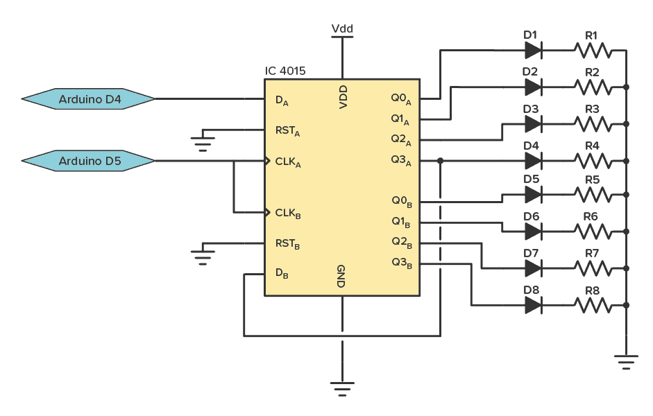
To build this circuit you’ll need:
- A 4015 chip, such as the CD4015BE
- 8 x Light-Emitting Diode (LED)
- 8 x 1 kΩ Resistor
- Arduino (Uno or any other)
In this circuit, you load 8 bits into the Arduino via the pins D4 and D5 (although any other pin would work too). After you’ve loaded the 8 bits, you’ll see these bits as either a lit LED (meaning a 1) or an unlit LED (meaning a 0).
Let’s say you want the last two LEDs to be on and the rest be off. Then you need to load the bits 00000011 into the 4015 IC.
To load one bit, set pin D4 to the value of the bit (1 or 0). Then set pin D5 HIGH, before setting it LOW again. Now you’ve loaded one bit. Repeat for the next 7 bits.
Technical Specifications
| Physical | |
| Case/Package | PDIP |
| Contact Plating | Gold |
| Mount | Through Hole |
| Number of Pins | 16 |
| Technical | |
| Direction | Unidirectional |
| Frequency | 17 MHz |
| Input Capacitance | 5 pF |
| Logic Function | Shift Register |
| Max Operating Temperature | 125 °C |
| Max Supply Voltage | 18 V |
| Min Operating Temperature | -55 °C |
| Min Supply Voltage | 3 V |
| Number of Bits | 4 |
| Number of Bits per Element | 4 |
| Number of Circuits | 2 |
| Number of Elements | 2 |
| Number of Input Lines | 1 |
| Number of Output Lines | 4 |
| Power Dissipation | 500 mW |
| Propagation Delay | 400 ns |
| Quiescent Current | 100 µA |
| Turn-On Delay Time | 400 ns |